Build your own FPGA
Posted by Nick Johnson | Filed under electronics, dfpga, open-7400
The Open 7400 Logic Competition is a crowd-sourced contest with a simple but broad criteria for entry: build something interesting out of discrete logic chips. It's now in its second year, and this time around I was inspired to enter it.
Discrete logic, for anyone who isn't familiar, are any of a number of families of ICs who each perform a single, usually fairly straightforward, function. Typical discrete logic ICs include basic logic gates like AND, OR and NAND, Flip-Flops, shift registers, and multiplexers. For smaller components like gates and flipflops, a single IC will usually contain several independent ones. As you can imagine, building anything complex out of discrete logic involves using a lot of parts; these days they're typically used as 'glue' logic rather than as first-class components, having been largely supplanted by a combination of specialised devices, microcontrollers, and FPGAs.
Building a microcontroller or CPU out of discrete logic is a popular hobbyist pursuit, and it serves a useful purpose: building a CPU from scratch teaches you a lot about CPU architecture and tradeoffs; it's an interesting and instructive exercise. So, I wondered, wouldn't building an FPGA out of discrete logic be similarly educational? Hence, my competition entry: an FPGA (or rather, a 'slice' of one) built entirely out of discrete logic chips.

Designing an FPGA from 7400s
The most basic building block of an FPGA is the Cell, or Slice. Typically, a slice has a few inputs, a Lookup Table (or LUT) which can be programmed to evaluate any boolean function over those inputs, and one or more outputs, each of which can be configured to either update immediately when the input updates (asynchronous) or update only on the next clock tick, using a flipflop built into the slice (synchronous). Some FPGA cells have additional capabilities, such as adders implemented in hardware, to save using LUTs for this purpose.
The core of a slice, the Lookup Table, seems nearly magic - taking an array of inputs, it can be programmed to evaluate any boolean function on them and output the result. As the name implies, though, the implementation is very simple, and it's a technique also used to implement microcode and other configurable glue logic. In principle, what you do is this: take a memory IC such as some SRAM or an EEPROM. Wire up the address lines to your inputs, and the data lines to your output. Now, any combination of input states will be interpreted as an address, which the memory will look up and provide on the data outputs. By programming the memory with the state tables for the functions you want to compute, you can configure it to evaluate anything you like.
Unfortunately, none of the 7400 series memories are manufactured anymore, and while there are plenty of SRAMs and EEPROMs available, the smallest sizes available are significantly larger than what we want for a simple discrete FPGA. Further, in order to be able to both program and read the memory, we'd need a lot of logic to switch between writing to the memory and reading from it (on a 'single port' memory, these use the same pins).
However, a simple solution presents itself: shift registers! A shift register is effectively an 8-bit memory, with serial inputs - convenient for our purposes - and each bit exposed on its own pin. By combining this with an 8-way multiplexer, we have a basic 3-input 1-output LUT. Our LUT can be reprogrammed using the data, clock, and latch lines, and many of them can be chained together and programmed in series. The 3 select inputs on the 8-way mux form the inputs to the LUT, and the mux's output bit is the output. So, in two readily available 7400 series ICs, we have one complete Lookup Table.

For our FPGA slice, we'll use two of these discrete LUTs, with their inputs ganged together. Why two? Because a combined capability of 3 inputs and 2 outputs about the smallest you can implement interesting things with. 3 inputs and 2 outputs lets you build a full adder in a single slice; any fewer inputs or outputs and just adding two 1-bit numbers together with carry requires multiple slices, which severely limits our capabilities.
The next component is the flipflops, and the logic for selecting asynchronous or synchronous mode. There's a profusion of flipflops and registers available, from 2 up to 8 in a single IC, and with various control methods, so that's no problem. Choosing between synchronous and asynchronous is a little tougher. The natural choice here is a 2-way multiplexer, but while chips with multiple 2-way multiplexers exist, they all gang the select lines together, meaning you have to choose the same input for all the multiplexers in a chip. Obviously, this isn't really suitable for our application.
Fortunately, a 2-way multiplexer isn't difficult to construct. There are several options, but the most efficient is to use tristate buffers. There are a couple in the 7400 range - the 74*125 and 74*126 that meet our requirements ideally. Each contains four tri-state buffers, the only difference between the two chips being that one enables its output when the enable line is high, while the other enables its output when it is low. By ganging these together in pairs, we can create multiplexers; one of each IC gets us four independent multiplexers. Two multiplexers, plus our register IC gets us our sync/async select logic. Of course, we need a way to control the multiplexers, so chain in another shift register to provide some state to program them with.

Now we've got the core of a basic slice designed, let's look at the second major component of any FPGA: routing. Flexible routing is a key attribute of any useful FPGA; without good routing, you can't get signals where they need to go and you waste precious resources, making your FPGA a lot less useful. Routing, though, uses a huge amount of resources to implement properly. What's the minimum we can provide and still get a useful and interesting result?
Typically, FPGAs position individual slices in a rectangular grid. Buses run between slices in the grid both horizontally and vertically. A slice is able to tap into some subset of the lines at its intersection, and can likewise output to some subset of the lines. Typically, the bus can continue through a slice uninterrupted, or the bus can be 'broken', effectively creating separate buses on either side of the slice. In some cases, buses can also be connected together in other ways, routing between different bus lines or between horizontal and vertical buses without the direct involvement of the slice.
One bit buses are a bit too narrow even for our purposes; a lot of interesting applications are going to require more than that, so let's see what we can make of 2 bit buses, both vertical and horizontal. Many FPGAs include a built in bias in one direction or another; this saves routing resources by favoring more common uses at the expense of making less common setups more expensive. In our case, we'll make it easier to read from the 'left' and 'top' buses, and easier to write to the 'right' and 'bottom' buses. We can do this by having 2-input multiplexers on each of the left, top and right buses; these multiplexers feed into our LUT's 3 inputs. For output, we can use more tristate buffers to allow one LUT to output to either or both of the right bus lines, while the other outputs to either or both of the bottom bus lines. To read from the bottom, or to drive the left or top lines, one simply has to drive the opposite side, and close the appropriate bus switch.
Speaking of bus switches, we'll go for the simplest configuration: a switch connecting each of the top and bottom lines, and a switch connecting each of the left and right lines, which can be opened or closed individually. The 74*4066 "quad bilateral switch" IC provides a convenient way to do this in a single IC. All of our routing requires state, of course - 3 bits for the input multiplexers, 4 bits for the output enables, and 4 more bits for the bus switches - so we'll use another shift register, and some of the spare bits from the one we added for sync/async selection.
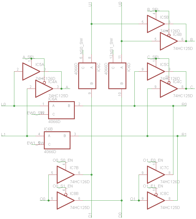
With routing done, we've more or less designed the entire of a basic FPGA slice in discrete logic. Let's take inventory:
- 4 x 74HC595 Shift Registers, for LUTs and routing/multiplexer state
- 2 x 74HC251 8-line multiplexer, for LUTs
- 2 x 74HC125 and 2 x 74HC126 Tristate buffers, for multiplexers and output enables.
- 1 x 74HC173 4-bit register, for synchronous operation.
- 1 x 74HC4066 Quad Bilateral Switch, for bus switches.
That's a total of 12 discrete logic ICs to implement one moderately capable FPGA slice. Add a few LEDs to give a visual indicator of the status of the bus lines, and some edge connectors to hook them up together, and we have a board that can be ganged together in a rectangular configuration to make a modular, expandable discrete logic FPGA. Pointless, given that it's a fraction of the capability of a moderately priced FPGA or CPLD chip? Probably. Cool? Most definitely.
Programming
Of course, it's no good having a DFPGA if there's no way to program it. We could figure out the bitmasks to achieve what we want ourselves, but that's tedious and error prone. Porting VHDL or Verilog to something like this would be tough, and massive overkill given the number of slices we're dealing with. Instead, I opted to implement a simple hardware description language, which I'll call DHDL.
DHDL doesn't attempt to handle layout or optimisation; instead it implements a fairly straightforward compiler to take logic expressions and turn them into slice configuration data. A DHDL file consists of a set of slice definitions, followed by a list of slices to 'invoke', arranged in the same manner as the DFPGA is laid out. Here's an example of a DHDL definition for a 'ripple carry full adder' slice:
slice adder {
  l0 ^ r1 ^ u0 -> r0;
  (l0 & r1) | (l0 & u0) | (r1 & u0) -> d0;
}
Here, l0, r1, etc, refer to bus lines - 'u', 'd', 'l' and 'r' for up, down, left, and right. The two addends are provided on l0 and l1; since the bus switches are closed, they're also available on r0 and r1, which the adder takes advantage of, since we can only select from one left bus line at a time. Carry input enters via the bus line u0. The first expression computes the sum of the two inputs and the carry, outputting it on r0. The second expression computes the carry output, which is transmitted to the next slice down via d0.
DHDL takes care of bus switch configuration for us here: by default, all bus switches are closed (that is, they conduct), but when we output to a bus line, the corresponding bus switch defaults to open. In this situation, that's the correct behaviour, since it allows us to read one of the addends on l0 and output the result on r0; it also ensures we separate the incoming and outgoing carry signals.
In some cases, we might want to configure the buses ourselves. We can use the expression `a b` to specify that a bus switch should be open, and the expression `a <-> b` to specify that it should be closed. Here's an example of a storage element that utilizes that:
slice storage {
  (u0 & r1) | (!u0 & l0) sync -> r0;
  l0 <-> r0;
}
This slice uses feedback to store a value, by outputting it on r0 and reading it back from l0. Since outputting to r0 would normally cause the compiler to open the switch between l0 and r0, we explicitly tell it that we want the switch closed, making the feedback possible. This definition also demonstrates how we specify synchronous vs asynchronous behaviour, with the `sync` or `async` keyword before the assignment operator. The default is asynchronous. Thus, this slice will output the stored value on r0 and l0; on the leading edge of a clock cycle where u0 is high, it will store the value of l1/r1 as the new value. Also note that since we're not outputting to d0, the switch between u0 and d0 is closed, meaning we could stack many of these vertically and control them all with an enable input. We've effectively created a flipflop slice.
Let's see what a complete FPGA definition looks like. Here's one for a 4-bit combination lock:
slice storage {
  (u0 & r1) | (!u0 & l0) sync -> r0;
  l0 <-> r0;
}

slice compare_carry {
  !(l0 ^ r1) & u0 -> d0;
}

slice compare {
  !(l0 ^ r1) -> d0;
  u0  d0;
}

storage compare,
storage compare_carry,
storage compare_carry,
storage compare_carry
First we define some slices - the storage slice we already saw, and a comparer, which outputs a 1 to d0 iff both the horizontal bus lines are equal and its u0 input was 1. We also define a version of the comparer without a carry, since the topmost slice will not have a carry input.
Operation is like this: To set the code, input the values on the l1 input of each of the leftmost slices, then take the top slice's u0 input high for one clock cycle. To test a combination, input the values on the l1 inputs again, but leave the top slice's u0 input low. The bottom right slice's d0 line indicates if the combination is correct.
Finally, let's try something a little bit more involved: a PWM controller. We'll need a counter, some comparators, and a set/reset circuit:
slice toggler {
  !r1 sync -> r1;
  r1 -> d0;
}

slice counter {
  r1 ^ u0 sync -> r1;
  r1 & u0 -> d0;
}

slice compare {
  !(l0 ^ r1) -> d0;
}

slice compare_carry {
  !(l0 ^ r1) & u0 -> d0;
}

slice overflow_pass {
  u0 -> r0;
}

slice srlatch {
  (r0 | u0) & !l0 sync -> r0;
}

toggler compare,
counter compare_carry,
counter compare_carry,
overflow_pass srlatch
The first two slice definitions, toggler and counter, collectively implement a binary counter. Toggler is the least significant bit, while any number of counter stages can be chained vertically to make an n bit ripple-carry counter - in this case, we've constructed a 3 bit counter. compare and compare_carry should look familiar from the previous sketch; they implement a ripple-carry comparator, in this case comparing the output of the binary counter with the other bus line, which will be set with switches. overflow_pass's job is very simple - it passes the overflow signal from the counter to its right output, making both that and the comparator output available to the final slice, srlatch. As the name implies, this is a simple set/reset latch, with the counter overflow resetting it, and the comparator setting it.
By setting the 3 input bits to reflect the duty cycle required, and pulsing the clock line sufficiently fast, the srlatch slice's r0 output will be PWMed with the appropriate duty cycle - which can be visually observed as the LED on that bus line being dimmed.
Fabrication
Designing and building this board was an interesting exercise. Due to the number of ICs and wanting to make the PCB as compact as possible, this was by far the toughest board to route that I've designed so far. Since I had time constraints to get the board sent off for fabrication in time for the contest, I ended up using an autorouter for the first time. Eagle's autorouter is remarkably awful, but it turns out there's a much better free alternative, called Freerouting. Freerouting is a Java based PCB router; it can import layouts from Eagle, KiCad and others, and exports scripts that can be executed to implement the final routing in your CAD tool. Where Eagle wanted to produce a board with over 150 vias, Freerouting was able to produce one that had fewer than 50, and visual inspection shows it to be fairly sane, too. It's not just for automatic routing, either - it has an excellent manual routing mode, where it'll allow you to nudge existing tracks around without having to rip them up and reroute them every time you need to fit another line in.
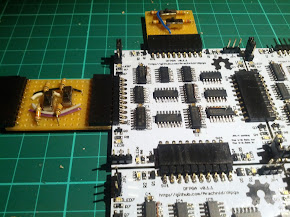
For fabrication, I went with the excellent Hackvana, who made me up 20 of the boards and had them to me in record time. A jumbo order of parts from Farnell/Element14 saw me sorted for parts, and all that was left was hours and hours of soldering - with over 200 SMT pads on each board, the assembly process takes a while.
Of course, as with any first iteration design, there were problems. A couple of minor design improvements occurred to me almost immediately, which would've increased the board's capabilities somewhat, and the jumpers that let you determine how the serial programming stream connects between boards could be better placed. More problematic, I accidentally tied all the shift registers' reset lines low, when they're actually active low - they should be connected to the 5v rail. After some experimentation, however, I came up with a greenwiring solution for this, which you can see in the photos below; it doesn't even add to the construction time by more than a couple of minutes per board. This bug is, of course, fixed in the schematics.
Demonstration
How does it look once assembled and working? Very cool. It may not be anywhere near as capable as a real FPGA, but it's also a lot easier to inspect and understand. With LEDs on all the bus lines you can see exactly what the internal state is at any time, which makes debugging a whole lot easier.
Here's one of the boards in the array fully constructed and hooked up; click the photo for more.
Of course, it wouldn't be complete without a video of the DFPGA in action...
Source
All the design files, along with the DHDL compiler, test suite, and demo definitions are open source under the Apache 2.0 license. You can find them all on Github here. If you decide to build your own DFPGA, or find the schematics or code useful in your own project - let me know!
Future developments
Remember how I rubbished the use of dedicated memory chips at the beginning, saying that all the ones available now are too big, and too difficult to interface with? Well... that's not quite as accurate as I thought when I was designing things.
It's true that the memory you can get is mostly larger than we need, but that can be an advantage in moderation - it means it's possible to construct much more capable slices. How would you like a slice with 8 inputs and 4 outputs, that can output to any of the bus lines, and has 4 bits of internal state, allowing it to implement a 16 state state machine in each slice? And all with a little over half as many ICs as the design above? It turns out that with a few clever tricks, that ought to be possible - with one catch.
The catch is this: the smallest SRAMs available are 256 kilobit, which is really quite large - so much so that an embedded processor like an Arduino could never program even one of these slices without external memory. We can use EEPROMS instead, which tend to be a bit smaller and could be easily programmed ahead of time, but that still leaves us needing a way to store the other configuration bits, such as the output enables. EEPROM shift registers, unfortunately, don't really seem to exist.
With a little clever optimisation, though, a compact design that loads the output enable state from the EEPROM at power on is possible, albeit somewhat more complicated than the current design. Unfortunately, I suspect the demand for discrete logic FPGAs - even fairly capable ones - is low, so it's unlikely this design will ever see the light of day.
I could be wrong, though. Do you want your own discrete FPGA? Can you think of a practical use for one? Let me know in the comments!
Previous Post Next Post